Canada’s Instrumentation Leader Since 1946.

Canada’s Instrumentation Leader Since 1946.

 Hoskin Environmental
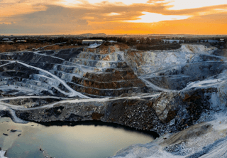
Sampling and monitoring instruments for air, water, weather and soil for the environmental, agricultural, mining and research markets.
 Hoskin Geotechnical
Materials and Product testing for soil, asphalt, petroleum, concrete, mining, cement, and research industries.

 Hoskin Instrumentation
Sensors, transducers and instrumentation for industry, manufacturing, research and development and factory automation.
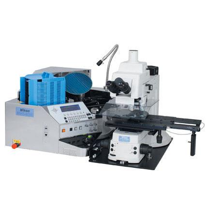
Nikon’s newest and most sophisticated wafer loader for IC inspection microscopes. The NWL200 series is the first lineup of wafer loaders for inspection microscopes capable of loading 100 micron thin wafers. Thanks to a new chuck system, the NWL200 series achieves highly reliable loading suitable for inspection of next-generation semiconductors. Improved wafer-sensing functions also help […]
 Contact us for details
The NWL200 series is the first lineup of wafer loaders for inspection microscopes capable of loading 100 micron thin wafers. Thanks to a new chuck system, the NWL200 series achieves highly reliable loading suitable for inspection of next-generation semiconductors. Improved wafer-sensing functions also help prevent damage to wafers, while wafer edge-chipping detection automatically detects edge-chipping defects.
With optional Edge-chipping detection, which was difficult with conventional wafer loaders for microscopes, can now be performed automatically. This enables macro inspections of all areas, adding to the support for inspection of pattern side, back side center, and back side periphery that was already available with earlier models. With high-precision automatic detection, edge defects that cause wafer cracking can be removed promptly.


Copyright - 2026 - Hoskin Scientific

